Implementation of the solar micro-inverter
Read below for how I built the working prototype array. There are PCBs available, and the schematics contain pretty much all parts you might need to build a working model. The firmware is even available on github. However, because this is a far from simple project, and because there are no assembly instructions, I suggest using this website as an educational resource. Take what I have done and build on it. Build your own awesome inverter, and tell me about it.
-Martin van den Nieuwelaar
The stages of the micro-inverter are as follows.
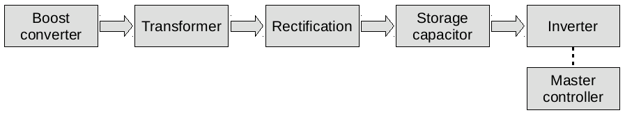
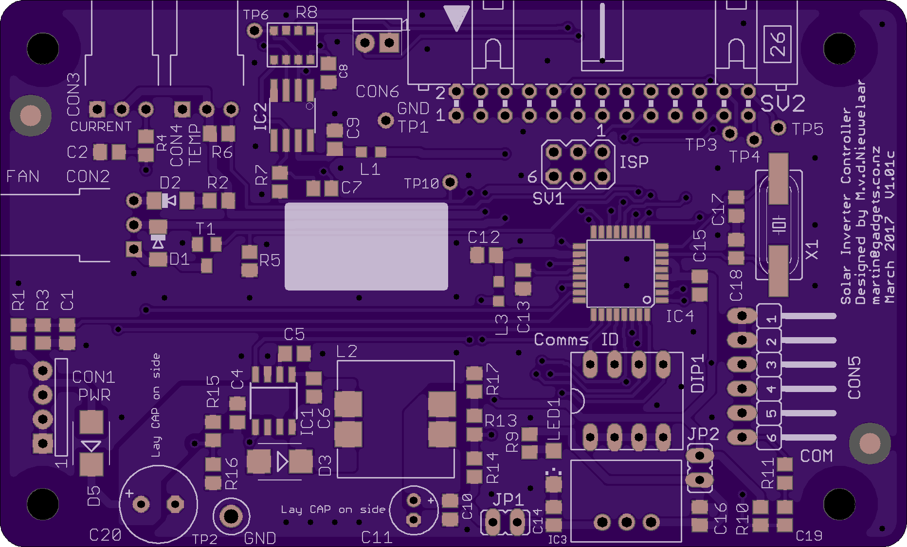
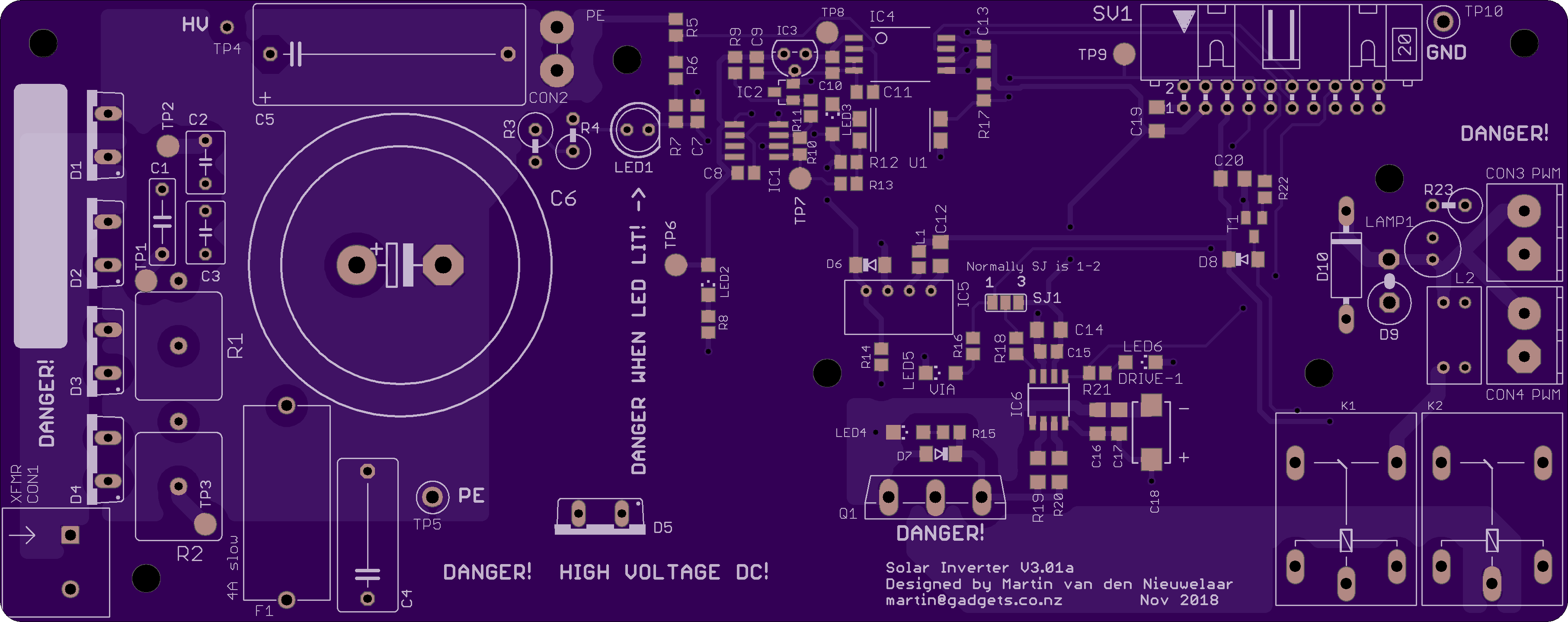
To actually build the micro-inverter I decided to split the design across multiple circuit boards (PCBs). This was done in an attempt to reduce the amount of work required if one part of the circuit did not function and it had to be re-designed. The downside with such an approach is that there ends up being more connectivity between boards meaning more connectors and wires. Still, for the prototype this approached worked well.
Expanding upon the first diagram, the next one shows how I broke things down by PCB.
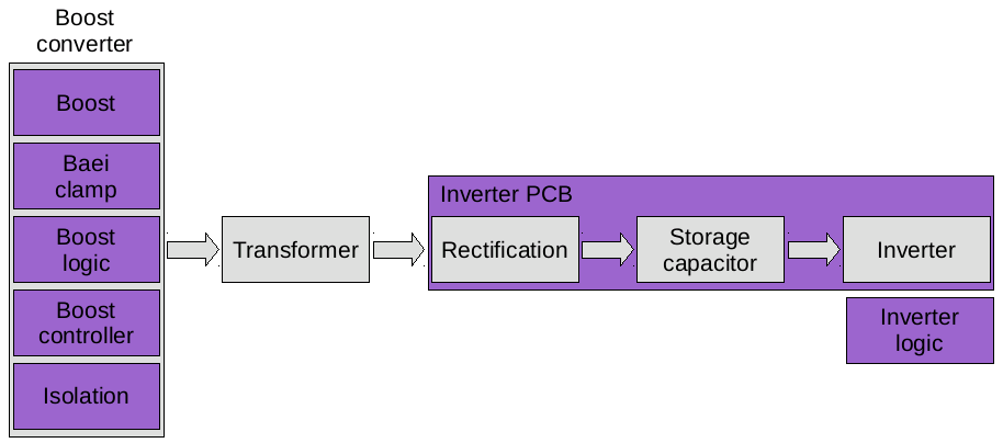
You will see that I broke the implementation of the boost converter into five separate boards. The demarcation proved to be quite successful and allowed the stacking of a number of boards which as an added benefit made effective use of the volume available.
The transformer was not mounted on a PCB and so it is shown separately.
The inverter PCB actually contains multiple stages: rectification, the storage capacitor and the actual inverter. While physically large (and hence expensive) this board does not have great complexity. The large size is due at least in part to the bulky size of the components and connectors.
An inverter logic PCB was also designed. This handles combining the timing logic from the master controller and the state of charge of the storage capacitor. It contains a few gates, a flip-flop and some de-glitch circuitry. This board stacks on top of the inverter PCB.
Boost
It will be easiest to understand the operation of the boost circuit by having the schematics at hand. I suggest opening them in a second window as the text will refer to them frequently.
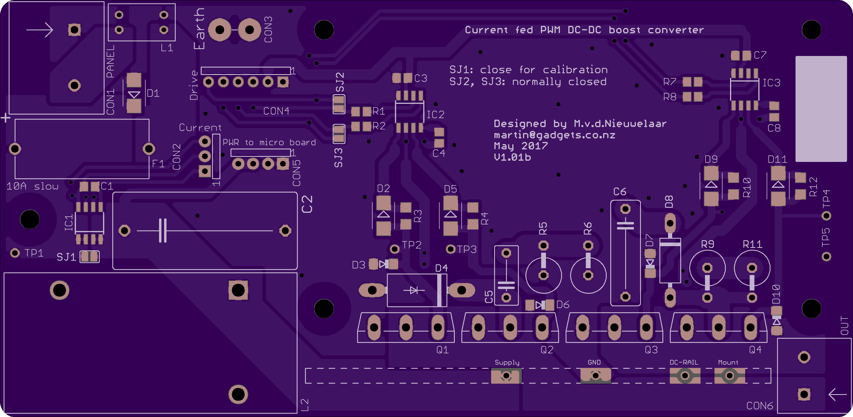
The photovoltaic panel connects at CON1. I use two 24V nominal panels wired in series giving 48V nominal. The panels are rated at 190W, so two together gives a 380W rating. At that peak power output one can expect just under 8A of current. The components in the boost converter are sized accordingly.
A common mode choke L1 is there to reduce RFI travelling from the converter back down the lines to the PV panels. F1 in combination with D1 provides some safety to connecting the converter to a supply using the wrong polarity. In such a case, and if the supply can source more than 10A the fuse should blow. This is good for when testing with a bench power supply. For the PV panels I have used they cannot source 10A and so all we can hope for is that the diode D1 will prevent the voltage from going far enough negative to destroy circuitry.
IC1 is used for measuring the current into the converter. Combined with the measurement of the voltage we can calculate the power consumed by the converter (or that generated by the PV panels, if you want to think of it that way).
The main part of the boost converter comprises L2 and Q1-Q4. C2 is there to even out the supply voltage in effect reducing ripple on supply line. The converter is similar to but slightly different from a regular boost converter. Like a regular boost convert it has two modes. The first mode is with the output side of the coil (L2) connected to ground. In this mode the current in L2 ramps up. In the second mode the output side of the coil is connected to the load during which the current ramps down. In this variation of the boost converter there are two ways to connect the load. One is with Q2 and Q3 switched on and Q1 and Q4 switched off. The other is with Q1 and Q4 switched on and Q2 and Q3 switched off. Both of these will result in the output from L2 being connected to the load (CON6) but each will result in different polarity. So the result at CON6 is a waveform of zero output followed by a positive pulse followed by zero output followed by a negative pulse. The duration of the pulses is directly related to the period the inductor (L2) is not being grounded. By varying the time the inductor is grounded versus the time the inductor is connected to the output (the so called duty cycle), we can change the amount the voltage is boosted.
While it will not yet be obvious from the boost converter schematic, the output will always be limited to about 130V. So the input to the boost converter is about 45V and the output from it is about 130V. A boost ratio of 2.9. This output is connected to a transformer with a turns ratio of 1:2.5 and this results in a voltage at the output of the transformer of about 325V.
It is worth mentioning at this point that high voltages can be deadly. If you have ever received a shock from a piece of electronic equipment due to your own stupid fault I would recommend against building high voltage equipment. High voltage equipment is most unforgiving. That means potential DEATH! Instead please go and play with Arduinos and 5V micro-controllers and live a long and happy life.
The drive for the gates of the MOSFET switches is provided by IC2 and IC3. These gate drivers have an LED style input, as in you drive them as if you were powering LEDs rather than a TTL input. I have found these to provide good noise immunity.
D4 is a transient voltage suppressor which is designed to clamp the output voltage of the inductor to something reasonable in the case where there is no load to the boost converter. This might happen in a fault condition for example. There is a question of how long this suppressor will survive in such a state, but it may be long enough for the fault to be detected and the converter to shut down.
R5, R6 and C5 form an RC snubber. Likewise C6, D8, R9 and R11 form a snubber. These were put on the board as possible options but I do not use them. Instead I use the Baei circuit (see later) which I have found to work much better than a snubber.
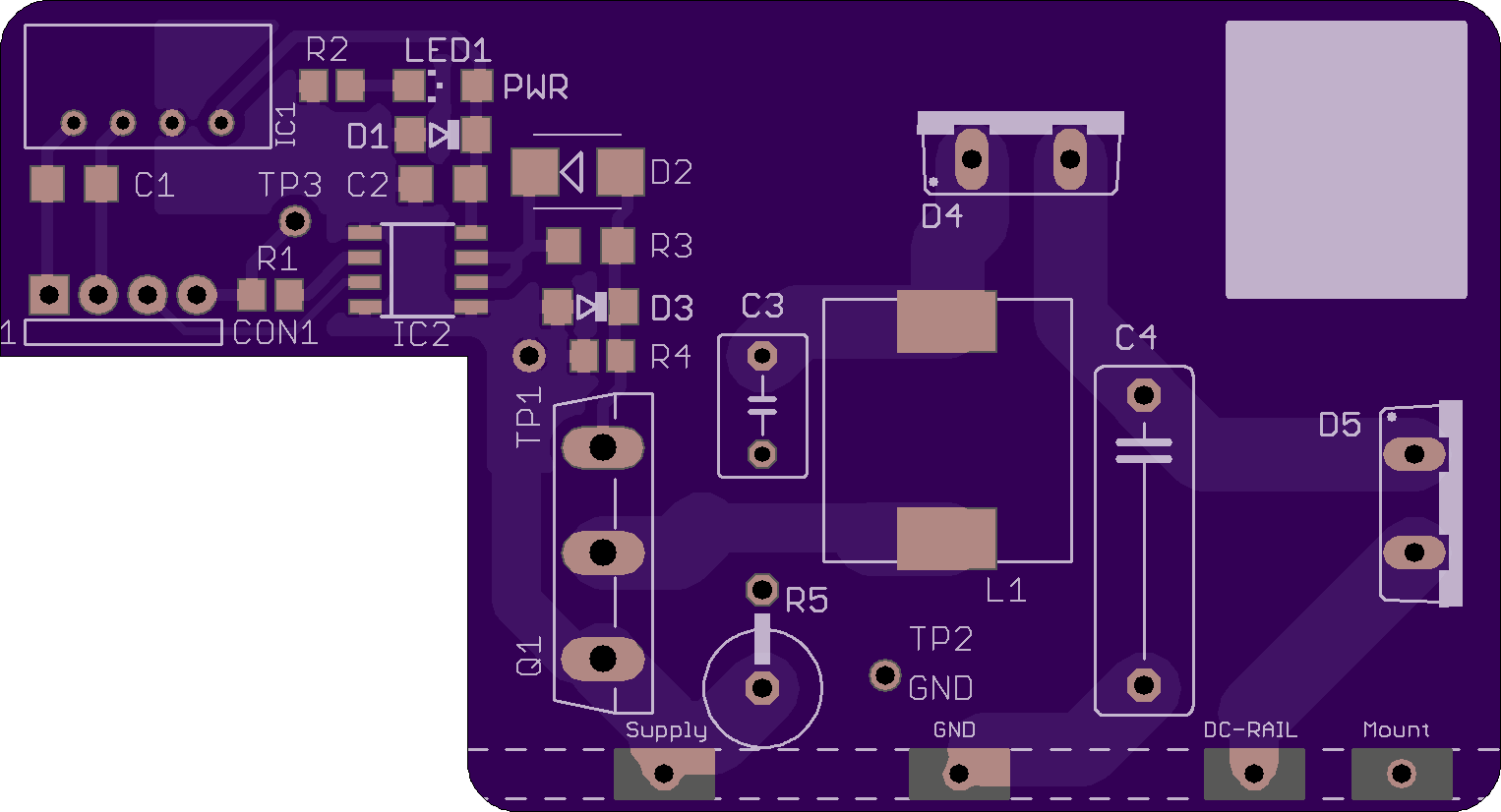
Baei clamp
The clamp board contains all of the parts required to implement the clamp, as well as the required isolated power supply and gate driver for the MOSFET.
The basic operation of the clamp is reasonably straight forward however the actual implementation involves some calculation to make it work well. Basically, for the boost converter (above), consider the transition between when the converter is powering the load, and when the converter is boosting. This transition involves turning on a pair of MOSFETs in order to connect the output of the inductor to ground. Without any extra circuitry such as clamps etc. in order to do this we would have to turn on the MOSFETs while there is still considerable voltage across them (about 130V). We can do this, but there will be some energy lost (as heat) as the MOSFETs turn on. If we can lose less energy (in the form of heat) our circuit will be more efficient. That is where the Baei clamp comes in. We turn on the clamp (Q1). The energy from DC-RAIL (which is at about 130V) goes through D5, D4, L1 and Q1 into the V-SUPPLY rail which is at about 45V. Because there is an inductor (L1), the current increases slowly. A nice side-effect of this is that Q1 turns on when there is zero current (zero-current switching or ZCS). Energy flowing through this path causes the DC-RAIL voltage to drop. While the MOSFET is on, current in L1 ramps up, but at some stage the DC-RAIL voltage will drop below V-SUPPLY. After this happens the current in L1 starts to decrease. The current in an inductor cannot stop immediately and so it keeps flowing, but the D4 end of L1 continues to drop in voltage to compensate until it reaches zero. It cannot go below zero. In effect L1 is used to drain DC-RAIL to zero Volts. This whole process doesn't take long to happen. Approximately 525ns in fact. Once DC-RAIL is at zero Volts the boost converter MOSFETs can be turned on. There is zero voltage across them and so they turn on efficiently (zero-voltage switching or ZVS). There is a fairly small time window where DC-RAIL is at zero Volts and so the timing is quite critical to achieve ZVS.
Note that the energy taken from DC-RAIL is not converted to heat, but is fed back into the input of the converter, to be used again. How cool is that!
At some point the clamp needs to be turned off but this timing is not critical. Basically the clamp is turned off (Q1 turned off) before the boost converter MOSFETs are turned off. There is no current flowing through Q1 and so it turns off efficiently with zero current switching (ZCS). The boost converter MOSFETs are then turned off. The voltage across them is zero when the are turned off and so they turn off efficiently (ZVS). After that the voltage on DC-RAIL will increase and any inductive spikes (which themselves are unwanted) that might normally occur in a boost converter flow through D5 into C4 effectively snubbing them. C4 will be drained next time the clamp turns on, so once again the energy does not convert into heat but instead is fed back into the input of the boost converter.
IC2 is a gate driver chip with an isolated LED drive input. IC1 is a DC to DC converter which provides an isolated power supply for driving the gate driver and the MOSFET itself. The whole circuit floats at V-SUPPLY hence the need for isolation.
An in depth discussion of the operation of the clamp can be found in the thesis of Mohammadjavad Baei A New ZVS-PWM Full-Bridge Boost Converter.
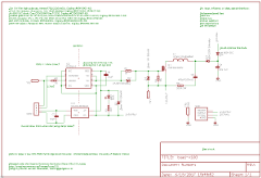
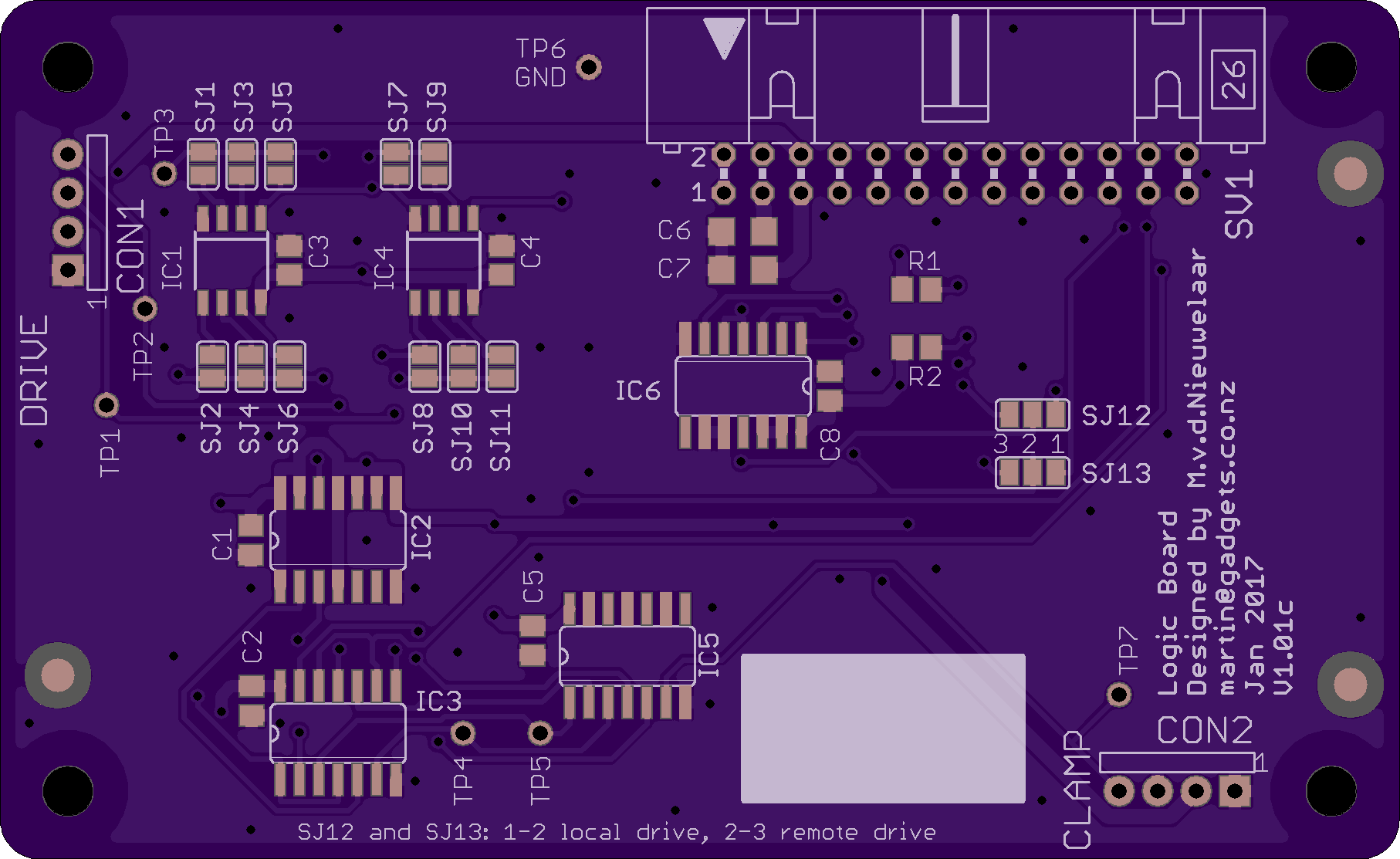
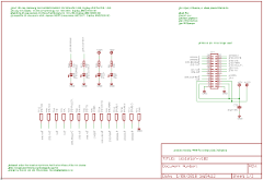
Boost logic
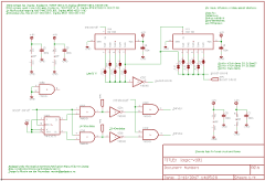
This board generates the timing signals to operate both the boost converter as well as the clamp. SYS-DRIVE comes from the micro-controller and is a 50kHz PWM signal. The pulse width dictate the duty cycle of the boost converter and hence the amount of energy transferred. IC4 and IC1 are used to create a delay in the range 500-1000ns. SYS-DRIVE drives the Baei clamp, and the delayed signal is then processed using IC2A, IC3A-D, IC5A, IC5B, to create alternating drives for each pair of MOSFETs in the boost converter.
Worth mentioning are SJ12 and SJ13. These offer two different types of operation of the inverter. In position 1-2 the micro-controller will generate timing for the inverter. This means the inverter can run stand-alone without a master controller. This is fine if you have just one inverter. If you have more than one inverter you need to synchronise the outputs from every inverter together and that requires the master controller. In this case the jumpers should be set 2-3.
Boost controller
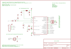
This board contains the micro-controller, an ATMEGA 328P. Those reading this who have not yet fallen into a semi-comatose zombie-like state may notice that this is the same chip used on many Arduino boards. Indeed, this PCB is Arduino compatible. That is to say it is not an Arduino at all, but I programmed it with the Arduino boot-loader and I use the Arduino IDE to program it. So if you are familiar with Arduino you will find working with the source code for the project quite straight forward.
DIP1 allows the setting of the inverter ID. Each inverter in an array must have a different ID. With four DIP switches there is the possibility to have up to sixteen inverters in one array.
Sheet two of the schematic shows the power supplies for both the 12V rail and for the micro. The 12V regulator can accept at most 76V on its input and so this is the hard upper limit of the voltage of the PV panels that may be connected. The 5V supply for powering the micro is generated from the 12V rail.
There is a fan drive output (T1) that can power a PC type fan, if you need it. 3-wire fans are supported and so it's possible to measure the RPM of the fan. In the prototype I built, I have used 60mm fans. Unfortunately this was necessary as the location I chose to install the array gets very hot. They are located under a PV panel on a hot tin roof. The roof gets skin-burning hot in summer. Ouch!
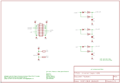
Sheet four has a balanced to single-ended converter. This takes a balanced line from the inverter that has a measurement of the voltage on the bulk storage capacitor. The balanced line has good noise immunity, but we need to convert it back to single-ended before the 328P micro can sample it on a single-ended analogue input.
Some of the schematics and source code for the inverter are now on github.
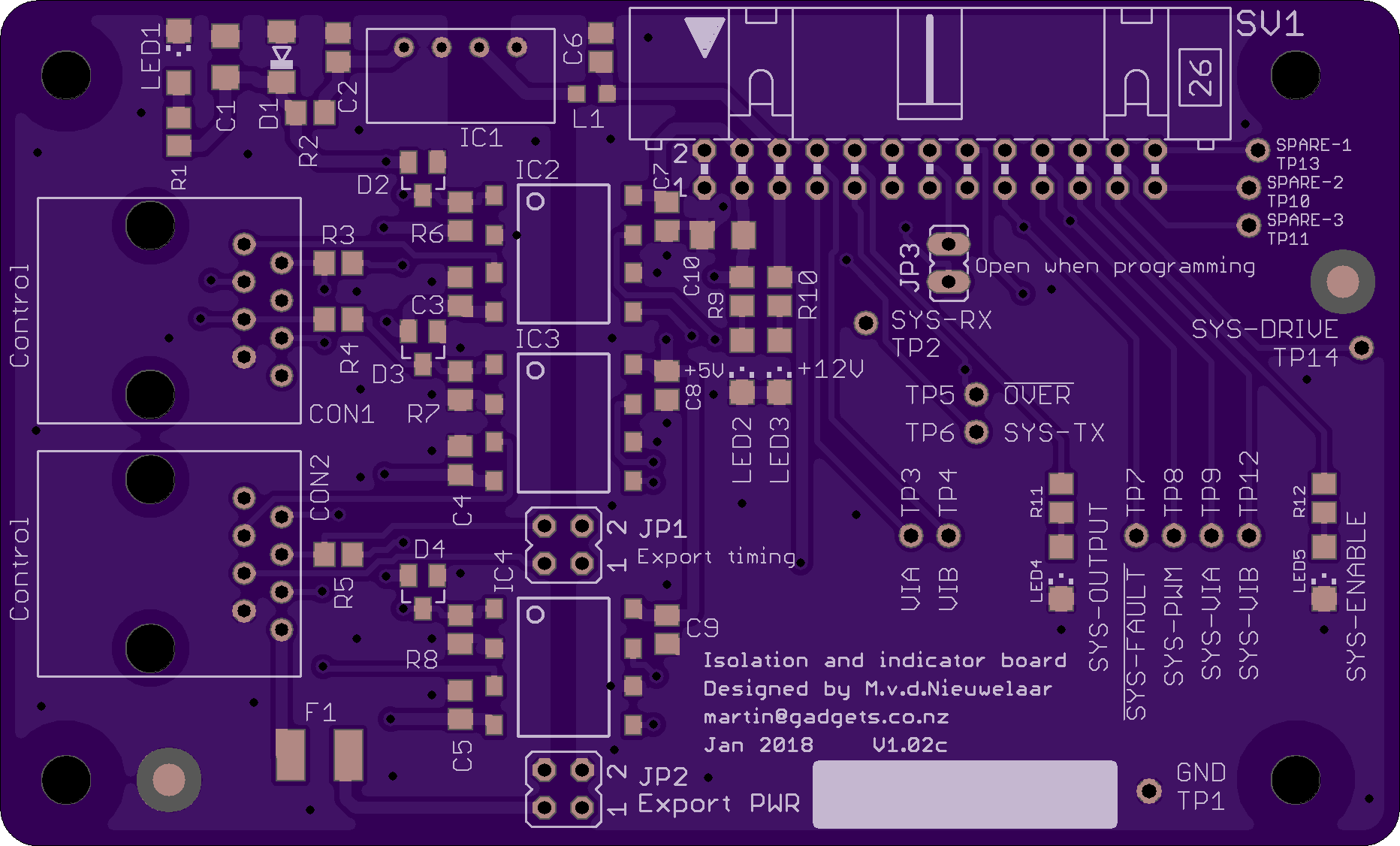
Isolation
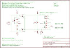
The isolation PCB connects the low level signalling of the inverter to the outside world while providing a degree of isolation. Particularly when connecting multiple inverters together it is important that they are allowed to float independently from each other. Inverters are then be daisy-chained together and connected to the master controller.
Each inverter has a transmit (TX) and receive (RX) line. This is used to provide full duplex communication with the master controller. Each inverter listens for commands (polls) from the master controller and will respond only if the poll is addressed to that inverter.
In addition to TX and RX there are two outputs from each inverter: FAULT and OVER. FAULT is used to signal a module fault that requires operator attention. OVER is used to signal that the voltage on the inverter storage capacitor has reached a high enough level to provide output. This is used for diagnostic purposes. Both of these outputs are of the open-drain type and work in a bus environment.
There are two further inputs to each inverter: VIA and VIB. These were originally used to generate a pseudo-sine wave output from the inverter, but that design was abandoned in favour of a simple pulsed DC output. Therefore only VIA is presently used.
By closing jumpers JP2 it is possible to export 12V power from an inverter onto the bus. This must be done at most on one inverter so that they don't fight each other. This exported power can be used to power the master controller. In this way the entire array works powered from sunlight and no plug pack or low voltage supply is required in order to run any of the system at all. This offers true resilience in case the power to your house should fail.
Inverter
Power from the output of the transformer enters the circuit at CON1. It is rectified by D1-4 and stored in the bulk storage capacitor C6. It is important that this cap is specified to handle both the ripple requirement of the inverter as well as the temperature in which the inverter will operate. There are various snubber components C1-3 and R1-R2 that have a place on the board but they are not required in practice. A string of resistors R3-7 step the voltage on the storage cap down to two different sense levels. Additionally and of significant practical use is the bright red LED1 which will glow when there is a significant voltage on the storage cap. When this glows it is an indication to keep away from the circuit!
I have mentioned already the danger of working with high voltages, but I will mention this yet again. Do not build this circuit, or any high voltage circuit for that matter if you are even slightly concerned about the risk of DEATH that high voltages pose. In particular, the high voltage DC that is present in the storage cap is LETHAL! Unlike the friendlier AC, DC does not give you a chance to let go, and so if you manage to get this voltage across your body the entire energy contents of the capacitor will discharge into you, which will likely cause your sudden demise. You have been warned, again! Maybe you consider mountaineering or free diving as a hobby instead?
On sheet 2, IC6 is the gate drive IC for the single MOSFET in the inverter. IC5 is an isolated DC to DC converter for powering the MOSFET gate driver as well as for the 5V power supply on the power side of the board. It is worth noting that the inverter has the low level signals isolated from the power side of the circuit.
On sheet 3, comparator IC1A is used in conjunction with opto-isolator U1 to produce a TTL output that is low (active low) when the voltage on the storage cap is high enough to effectively use. That is to say about 310VDC.
On sheet 4, IC4 is used to measure the voltage on the storage cap. This chip generates a balanced and hence noise immune signal that is output to the micro-controller. It has its own 5V power supply generated by IC3.
Sheet 5 shows the switched power path for the power coming from the storage capacitor. The storage capacitor is connected to DC-RAIL and this goes through fuse F1. This is a sand filled fuse capable of breaking the circuit should something go horribly wrong. Q1 is used to actually switch the flow to energy to the load. D5 is used to make sure that no energy flows back into the storage capacitor. This could potentially happen when multiple modules are connected in parallel and so D5 prevents this.
The output from the inverter is enabled or disabled on sheet 6 by relays K1 and K2. These are extra safety measures to make sure that the output is disconnected when the board and hence the relays are powered off. Without these another inverter in the array could end up at least being galvanically connected when we were perhaps not expecting it. L2 is a common mode choke intended to reduce RFI on the possibly long power line that connects the inverter to the load. D9 is a transient voltage suppressor and it is there to prevent the inverter producing excessively high voltages in a fault condition. If triggered, fuse F1 should blow. LAMP1 is a visual indication that power is being generated; a neon tube! D10 absorbs the inductive kickback from the load. It keeps the output waveform looking nice and square, and it doesn't get warm in practice. Two outputs CON3 and CON4 are provided so that the high voltage side can be daisy-chained to other inverters.
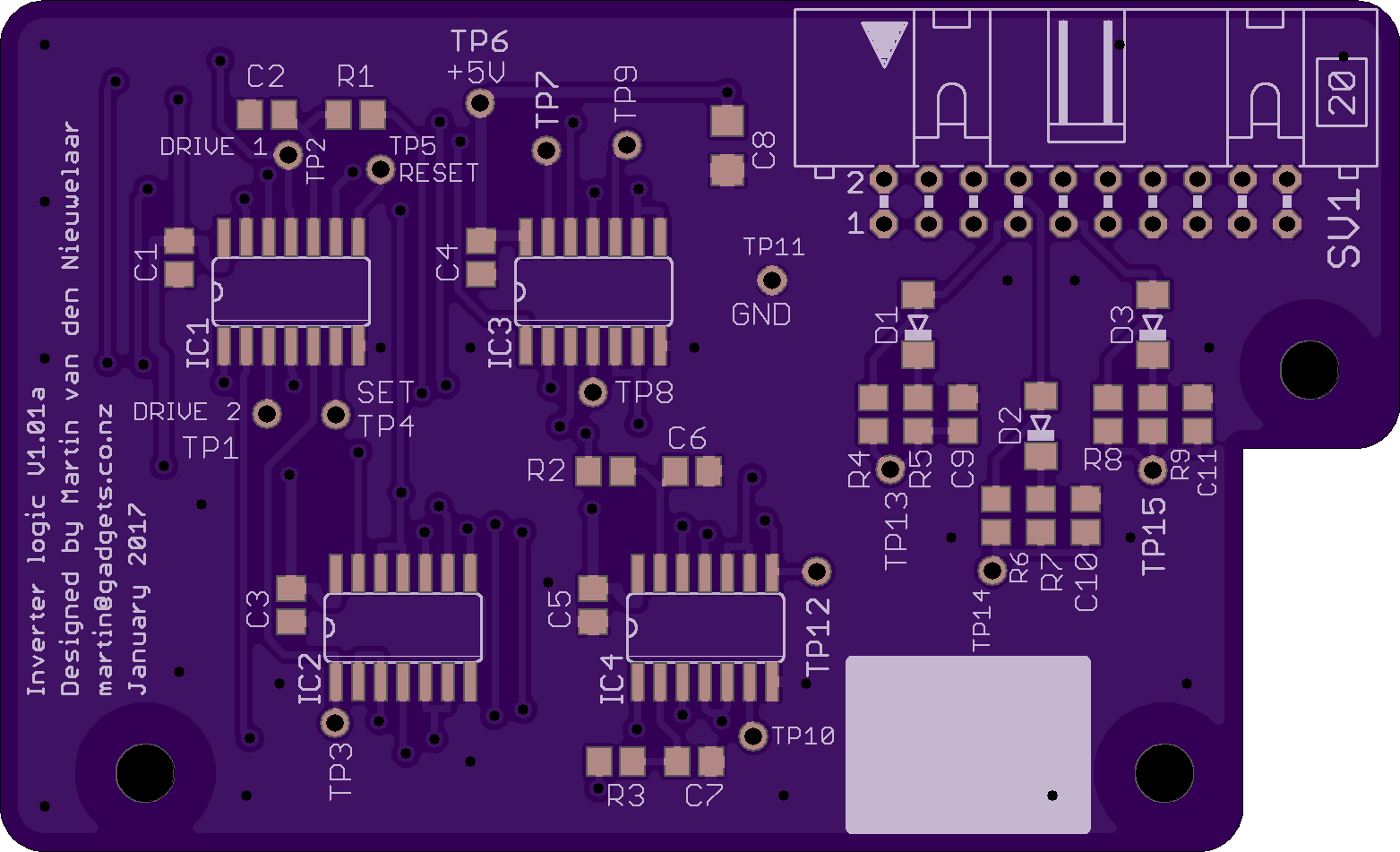
Inverter logic
Please note that VIB is obsolete and no longer being used.
The switching of high voltages and the resulting interference caused was a big problem in early prototypes. The interference appeared in all sorts of unwanted places. The OVER, VIA and VIB signals are passed through low pass filters (Eg. D3, R8, R9, C11) in an attempt to filter out some of this interference.
Sheet 2 takes the 100Hz 50% duty cycle timing provided by the master controller, combines it with the signal saying whether there is enough voltage on the storage cap and produces a 100Hz timing with a duty cycle matching the load to the energy flowing into the storage capacitor. That may need some further explanation.
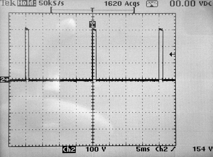
Consider that the boost converter is running optimally and is therefore taking whatever power is generated by the PV panel and putting it into the storage cap. This is how the boost converter operates, and that's all it does; power from PV, put it into the storage cap. Well, there are a few other things it does, but that's the basic stuff. Now, in steady state whatever energy goes into the cap must come out of the cap. We know this is true because if more goes in than comes out the cap will eventually explode by going over voltage. Similarly if more comes out than goes in, the cap will end up with zero Volts on it and, well, that's no use either. So whatever goes in, comes out. Now, we know that we want our output waveform to be a 100Hz variable width pulse of about 325VDC. This will be a good match to a 230V 50Hz AC heating element of the type used in a hot water cylinder. So given we want 100Hz output and 325VDC in amplitude, the only thing we can play with is the duty cycle. By varying the duty cycle we can either take a little bit of energy out of the storage cap, or a lot. The circuit on sheet2 produces DRIVE-1 for the inverter MOSFET with a duty cycle exactly matching what is required in order to keep the voltage in the storage cap above about 310V.
I don't have a photo showing 100Hz output handy, but here is the waveform when I was testing with 50Hz. Note the slight downward slope of the top of the waveform.
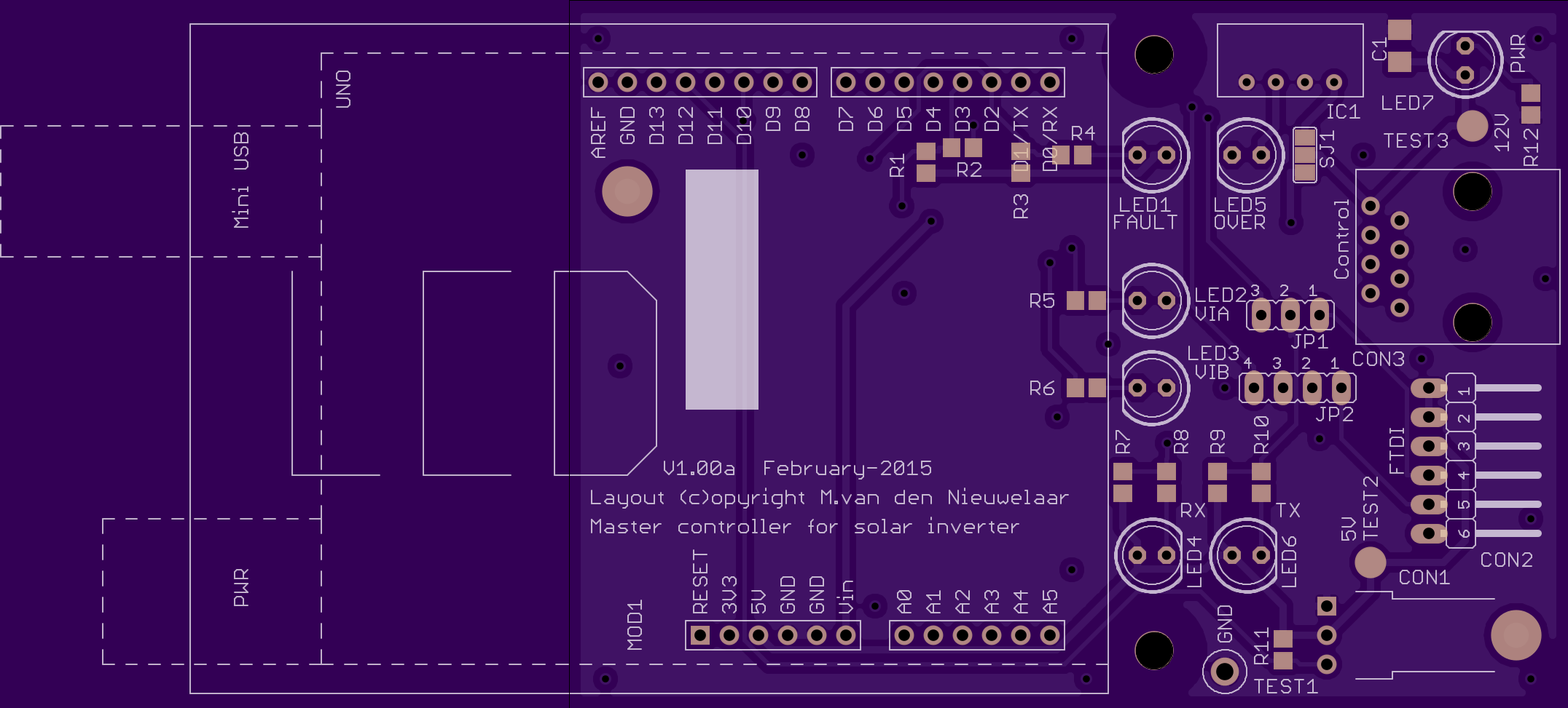
Master Controller
The master controller provides the 100Hz signal used to synchronise the output of all the inverters in an array. It is required if you have more than one inverter, if you need to measure the temperature in the hot water cylinder, or if you want to be able to interact with the single inverter you do have. So in many cases it will be desired, if not required.
The circuit board is sandwiched between an Arduino UNO which provides the compute power, and an Arduino compatible LCD 16x2 LCD display with keypad. These LCD and keypad combinations are available from many places only for just a few dollars. The circuit connects to an LM35 temperature sensor which is ideally placed in the sensor pocket at the top of the hot water cylinder. If you do not have a sensor pocket it should be possible to mount the sensor at the same place where the safety thermostat is located on the hot water cylinder. This sensor is used to monitor the temperature in the tank and to prevent it going over temperature. If the temperature goes too high the tank may fail, which would be a very bad thing indeed. For the prototype in addition to having the temperature sensor, which will turn off the inverters when the tank reaches 85 degrees C, the power wiring is additionally run through a fail-safe thermostat on the tank itself. So if the tank gets too hot, the high voltage pulsed DC circuit will open. The resulting lack of a load will cause the voltage on the caps in each inverter to go up and the resulting over voltage situation will cause each inverter to turn off.
The master controller board also provides visual indication of the FAULT status from each inverter at well as the OVER voltage status.
Another warning! Playing with the 230VAC power around a hot water cylinder can be deadly! If in doubt get someone who is qualified who can assist with this wiring.
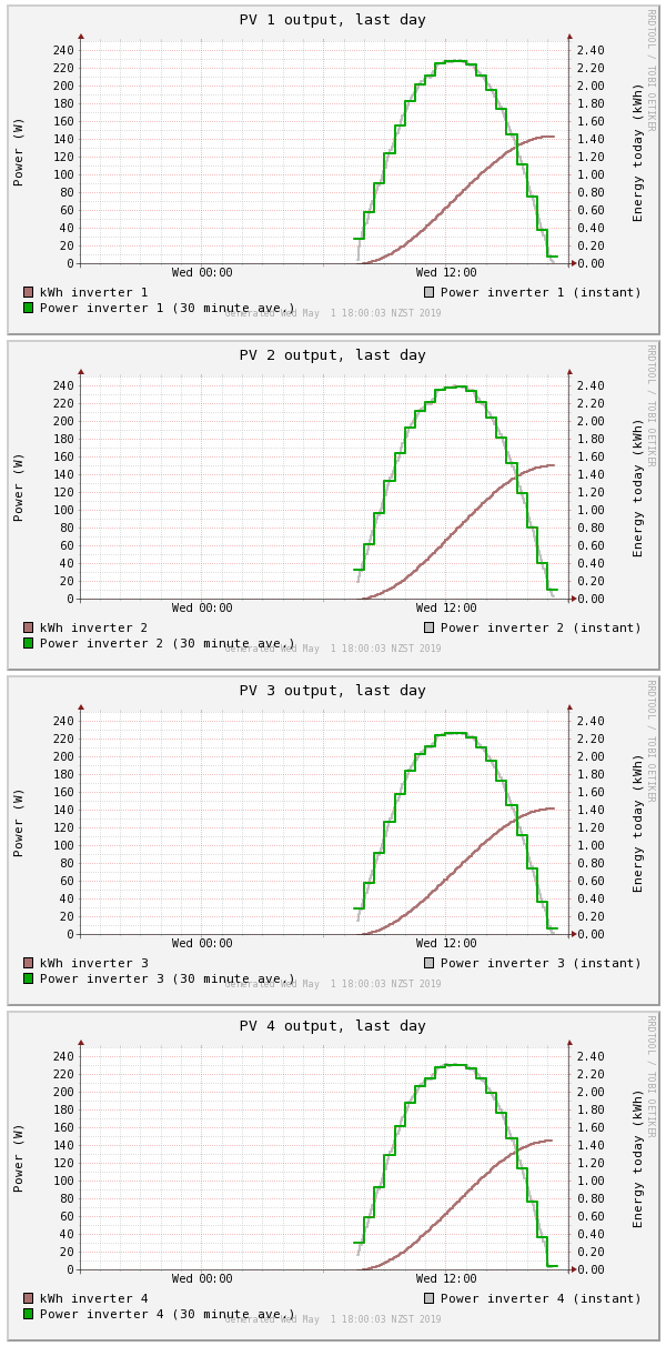
Output from the array
Below are graphs showing the output from the four modules on a textbook sunny day without a single cloud in the sky.
-Martin van den Nieuwelaar
This page is covered by the GNU Free Documentation License
Martin van den Nieuwelaar, martin at gadgets dot co dot nz
Last updated 12 May 2019
